 |
How ICID Works |
|
|
|
How ICID Generates a Unique ID from Device Mismatch What ICID cells do ICID (Integrated Circuit IDentification) is a small cell, made with standard digital CMOS processes and design rules, that produces a unique serial ID bit string from pairs of mismatched FETs. Mismatch is inherent in the CMOS process, and different for every pair of devices. An array of hundreds of pairs in each ICID cell, observed with a low-offset comparator, is serially accessed by counters from the system supplied clock. No programming or special processing is required; just build the cell, and read it out with a digital tester. MOSFET physics and voltage offset
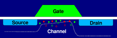
This is a cross section of a Metal Oxide Semiconductor Field Effect Transistor (MOSFET). If this is an N channel MOSFET, or NFET, then a positive voltage on the gate attracts electrons into the channel between source and drain, and the NFET conducts current. The minimum voltage necessary to establish strong conduction between source and drain is called the threshold voltage. The threshold voltage is determined by the materials that make up the FET, and the amount of positive and negative doping atoms in them. The threshold voltage is adjusted during manufacturing by adding or subtracting dopants to the channel area of the FET. The processes that put the dopants into the silicon - deposition, ion implantation, and diffusion - are random. Averaged across a whole wafer, the number of doping atoms is precisely controlled. But modern transistors are so small that the number of dopants in the channel of an individual transistor is a relatively small number, and this small number can fluctuate from transistor to transistor. These fluctuations result in fluctuations in channel charge, and result in fluctuations in threshold voltage. As processes are scaled down, the voltages in the devices are scaled down, too. The threshold voltage is reduced. However, the smaller transistors mean that their channels contain fewer dopant atoms. The statistical variation of N items is proportional to the square root of N over 2; the ratio of variation to average goes up as N is reduced, so the fluctuation of threshold voltage increases as devices are scaled down.
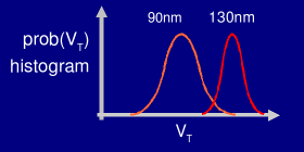
The voltage threshold for many devices can be plotted as a probability histogram, which looks like a Gaussian or bell curve. Most devices cluster near the average, but a few deviate widely from average, plus or minus. As the process is scaled down, the amount of variation compared to the average scales up. This is a big pain for digital device designers - the devices with low thresholds leak a lot, and the devices with high thresholds are slow. The leakage increases power, and the whole circuit is slowed down by the slowest transistor. Process designers are working hard to reduce the variation by clever use of materials, but it is unlikely they will ever eliminate variation. Systematic variation in analog circuits is reduced by using two FETs with sources connected together, feeding the input voltage between the gates, and measuring the current difference between the drains. This is called a differential pair, and is widely used in analog MOS circuits. Most disturbances of threshold voltage - temperature, bias levels, aging - tend to affect both FETs equally. The threshold voltage difference between the FETs - the offset - becomes mostly a function of channel doping, and is relatively insensitive to other variations. Pairs with positive voltage offsets tend to stay positive, and negative stays negative, for large variations in biasing and temperature.
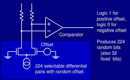
ICID measures the offsets of an array of hundreds of differential pairs. A counter selects one pair at a time. Each pair is biased so that the offset voltage is turned into a differential offset current, which makes a differential voltage on a pair of load devices. This differential voltage is measured with a high precision, low offset comparator, and turned into a binary one or zero. Since the offset of the device pairs is relatively stable, so are the bits produced by the comparator. Since the device pairs in the ICID array are small, a relatively small array can contain hundreds or thousands of them, producing many random bits in a small area. The good stuff The pairs in the array generate more variation if they are minimum size, so smaller ICID cells are better. ICID arrays scale linearly with the process. This is unlike EEPROM devices, fuses, laser-cut links, and other ID technologies, which cannot be easily scaled due to physical limitations. ICID gets better as processes scale down; other ID technologies get worse. The not-so-good stuff Because ICID uses differential pairs with a continuous variation centered on zero volts, some of the pairs will be very close to zero offset. Thermal noise, temperature changes, and bias changes can push a measurement from zero to one. This is called drift. As many as 1% of the bits may drift due to thermal noise. But the worst drift is due to temperature variation - 1% of the bits may drift for every 10C change in die temperature. This means that a device with 224 random bits, heated 60C between measurements, will have 14 changed bits between the two measurements. But that is the average number of bits changed; one out of a million devices may see as many as 40 bits change with a 60C temperature difference. But it does get better Generation 4 ICID cells incorporate many enhancements to reduce temperature drift, and to enable the system to select bit pairs that are less likely to drift. Combined with Hamming distance methods to compare identities, the chance of an identification failure becomes vanishingly unlikely. With a 224 bit ICID cell, misidentifications are reduced to the low parts per million, even among populations of billions of cells.
|
© 2007 by SiidTech, Beaverton, Oregon, USA. Page last modified Mon Feb 18, 2008 16:00 webmaster